
Transformerless Modified Sine wave Inverter Circuit
In this post we are going to construct a transformerless inverter circuit which can be power via solar panels and also using batteries. The proposed transformerless inverter design is a modified sine wave type which is better than square wave counterpart. We will learn the different stages of this inverter in-depth.
We will see:
- Full Circuit Diagram.
- Stages of this Transformerless inverter circuit.
- Difference between Square wave and Modified Sine Wave.
- How to test this Transformerless inverter circuit.
- Advantage and Disadvantage of this inverter circuit.
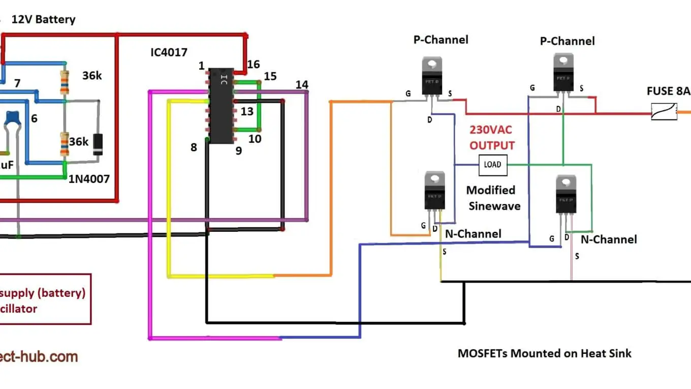
Transformerless Inverter Circuit Diagram:
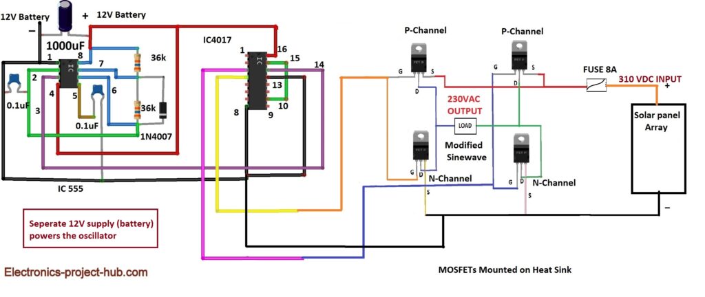
Circuit Description:
The circuit consists of commonly available components like IC 555 and IC 4017 and some passive components like resistors and capacitors. The IC 555 and IC 4017 constitute the oscillator stage which outputs modified sine wave. The MOSFETs does the job of switching the high voltage which is configured as H-bridge. The MOSFETs are rated above 400V which can drive 230V load without any issue. Since this inverter doesn’t boast a transformer unlike traditional inverters which can step-up the low voltage, we have to apply 310 VDC to the MOSFET stage. The MOSFETs will convert the high voltage DC to nominal 230 VAC, the waveform and frequency is determined by the oscillator stage.
Now let’s learn how each stage of this inverter functions in-depth:
The proposed inverter has 3 stages:
- Oscillator stage.
- MOSFET / Switching Stage.
- Power Input Stage.
These three stages will determine the output frequency, voltage and the quality (wave form).
Oscillator Stage:
The frequency and the wave form are determined in this stage. The IC 555 and IC 4017 combinedly make the oscillator stage and IC 555 is the heart of this project as it generates the pulse for the inverter. The IC 555 generates square pulse at 200Hz at pin #3; the frequency is determined by the network of RC component connected to IC 555. We can also see a diode connected across pin #6 and #7; this is for generating pulse at 50% duty cycle.
The role of IC 4017 is to convert the square wave generated by IC 555 to 50 Hz modified sine wave. Let’s have a look at how a modified sine wave looks like compare to square wave.
Square wave:

Modified Sine wave:
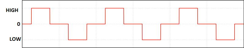
The modified sine wave is technically a better waveform than square wave and it is less noisy. Modified sine wave is used in many cheap commercially made inverters to power home appliances, but this doesn’t mean that modified sine wave is perfect.
Calculation of IC 555:
To get the desired frequency of 50Hz, the IC 555 has to generate 200Hz and the IC 4017 must divide the wave from by four. The IC 4017 can divide the wave form without any external components. To get 200Hz and 50% duty cycle from IC 555, we can use the frequency formula:
F = 1.44 / (R1 + R2) x C
F = 1.44 / (36000 + 36000) x 0.1 x 10^-6
F = 200Hz (exactly)
So, using two 36K resistor and 0.1 microfarad capacitor we got precisely 200Hz.
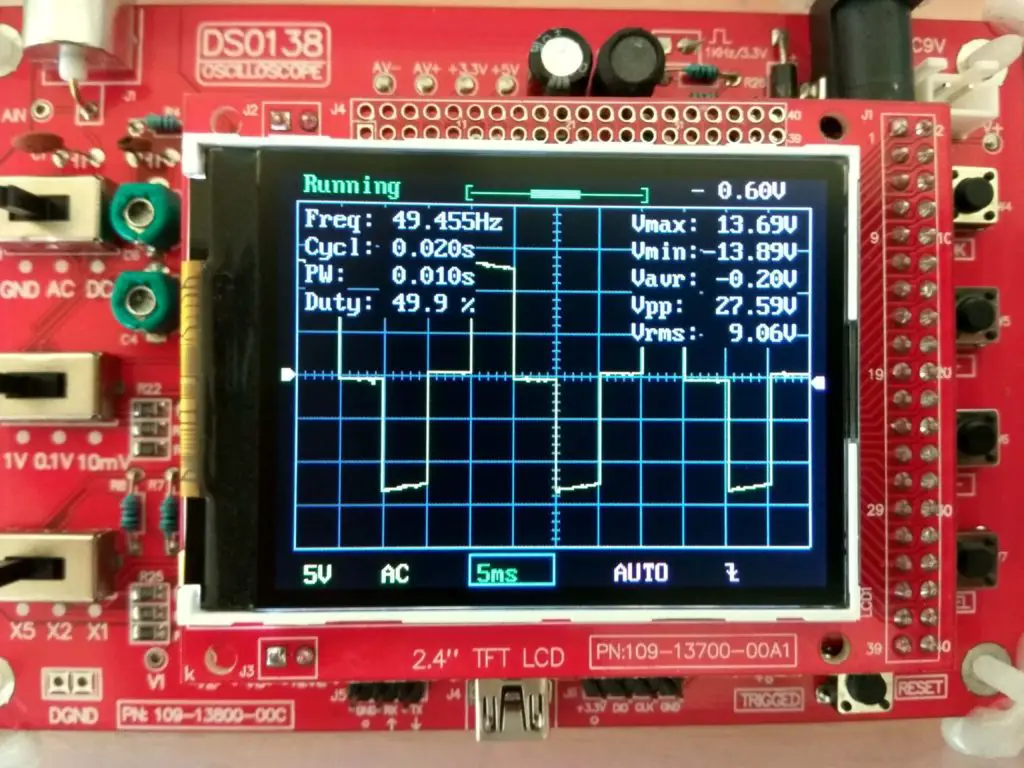
Let’s check the same using an oscilloscope at pin #3 of IC 555:
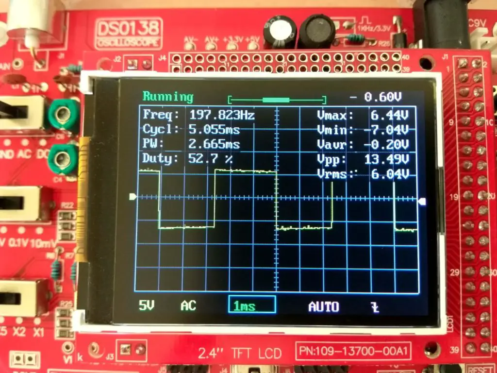
We got 197Hz and 52% duty cycle which is close enough; the slight variation is due to the tolerance of the resistors and capacitor.
Now let’s convert this square wave into modified sine wave using IC 4017.
Pin configuration of IC 4017:
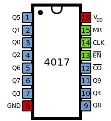
IC 4017 is a decade counter which can count from Q0 to Q 9 (10 outputs). For successive pulses applied at pin #14, successive outputs (Q0 to Q9) gets high. Here we don’t need all the 10 outputs, we just need 4 outputs so that we can divide the 200Hz input to 50Hz output.
To enable only four outputs we have connected the reset pin #15 to pin #10 (Q4 – 5th output), by doing so we are disabling outputs Q4 to Q9. Now the outputs get HIGH and LOW from Q0 to Q3 (First four outputs).
Out of the four outputs we are utilizing only 2 outputs which give the modified sine-wave shape. In the wave form we can see couple of pauses at 0V twice in a cycle this is because of the unused remaining two outputs which ultimately gives the required waveform.
Now let’s hook the oscilloscope and see the waveform at the outputs of pin# 3 and #4 of IC 4017:
As we can see, we got the exact anticipated waveform at 50Hz and 50% duty cycle. Now this waveform need to be amplified, to do this in the next stage we are using some powerful MOSFETs which will drive the connected 230VAC gadgets.
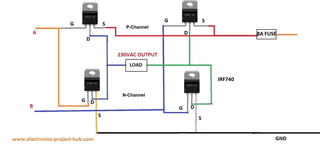
MOSFET / Switching stage:
In this stage the generated weak signal from the oscillator gets amplified. We are using 4 MOSFETs, two N-channels and two P-channels in H-bridge configuration.
H-bridge is the best way to alternate the polarity (converting DC to AC) across the connected load. To do this we need to switch the four MOSFETs in the following sequence.
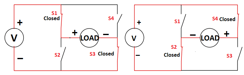
Now let’s consider the diagram on left side, the S1 and S3 (MOSFETs) are closed, now look at the polarity across the load, on left we have +Ve and on right we have -Ve. Now let’s open these two switches (MOSFETs) and close S2 and S4, now the polarity cross the load is reversed (diagram on the right side). To get 0V across the load, we just open all the MOSFETs, this sequence will repeat.
Alternate H-bridge configuration:
You can also build an H-bridge using 4 N-channel MOSFET with bootstrapping. Please note that BC547’s pins are flipped horizontally for drawing convenience, the transistor’s flat surface should face away from you in real life.

Specifications of MOSFETs:
IRF740 N-Channel MOSFET:
- Voltage Drain to Source (Vds): 400V
- Voltage Gate to Source (Vgs): +/-20V (Max)
- Continues Drain Current: 10A (Continuous)
IXTP10P50P P-Channel MOSFET:
- Voltage Drain to Source (Vds): -500V
- Voltage Gate to Source (Vgs): +/-20V (Max continuous)
- Continues Drain Current: -10A (continuous)
The MOSFETs used here can handle voltage as high as 400VDC and 310VDC from solar panel should not be an issue for these MOSFETs. If you could not find MOSFETs of these part numbers, you may utilize any other N and P channel MOSFETs with similar specifications.
Power Source:
The power source we are going to use is arrays of solar panels, the combined series output voltage around of 310 VDC. You can also use bank of batteries to get similar voltage level.

You need to get help of professionals to install solar panels. In real life solar panels are not directly connected to an inverter, they are installed with batteries with battery management system.
Why do I need around 310 VDC input to get 230 VAC output?
The modified sine wave need 310V peaks to get 230VAC RMS output. Ok, what do I mean by that? If you hook an oscilloscope to AC mains of our home, you will see that peak to peak voltage is 325VAC and not 230VAC.
The 230VAC is called the RMS (root mean square) and 325V is called peak to peak voltage. The RMS is the average voltage, since the voltage is varying with time from 0 to 325V and vice-versa; we cannot conclude a voltage measurement at any given instant. So, we are measuring the average voltage of the AC sinusoidal cycle, our multimeters and volt meters designed to measure RMS.
This is same for modified sine wave; we need around 310V peaks at 50Hz to get average of 230VAC.
But in the case of square wave the RMS = Peak voltage, meaning if we apply 230 VDC to the input we will get 230 VAC RMS. You can learn about such square wave transformerless inverter here.
How to Test this Transformerless Inverter Circuit:
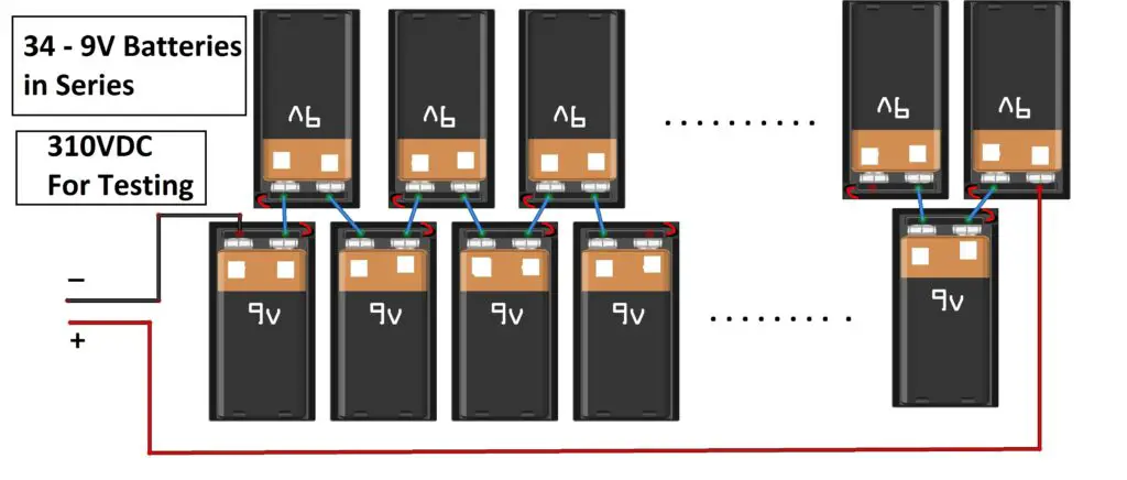
Once you complete the construction of this inverter circuit, you need to connect the oscillator to a 12V power source. You also need a high voltage DC source which can output 310 VDC, you may use high voltage DC lab power supply or you can connect 34 nine-volt batteries in series to obtain 310 VDC as a cheap testing solution.
Connect a tungsten bulb of 40 watt across the output terminals of the inverter, power the oscillator first and connect 310 VDC to MOSFETs second. As soon as you connect the high voltage DC to MOSFETs, the bulb should glow instantly at full brightness. Now your inverter is working fine.
How much power can it deliver?
From our estimation, it can deliver about 1000 watt or 1KW with MOSFETs cooled adequately. You need to apply 310VDC at 4A or above from solar panel / batteries to this inverter.
Pros of this inverter:
- Simple design with reasonable output quality.
- High Efficiency as the loss due a transformer doesn’t exist.
- Dirt cheap price to construct and zero maintenance for the inverter.
- It can power most of the home appliances.
Cons of this inverter:
- Need High voltage DC as input.
- Modified sine wave is not suitable for medical equipment.
- Installing solar panels and battery banks are expensive.
- No automatic voltage regulation is present to stabilize the output AC.
If you have any questions regarding this project, comment your questions, you can anticipate a guaranteed reply from us.
Blogthor
My nick name is blogthor, I am a professional electronics engineer specialized in Embedded System. I am a experienced programmer and electronics hardware developer. I am the founder of this website, I am also a hobbyist, DIYer and a constant learner. I love to solve your technical queries via comment section.


Can a circuit to stabilized the output voltage be added?
Yes, you can….
Sir/ Madam, would it be possible for me to use (1) 12v battery? Would it work in this manner:
For the oscilliator+bootstraping stages AND THEN using a basic 2-mosfet based power inverter circuit, turn the same 12v dc to ac, then step it up via a normal transformer with secondary as input and with primary as output, maybe even add a voltage doubler diode ladder. Thereafter, i rectify the output, filter it, the feed it as the 440v for the load?
Yes, the idea could work in theory but the mentioned MOSFETs can’t handle 440V load and the voltage doubler stage may not provide enough current to the load.
Hello.
How this circuit can be modified in order to incerase the power up to 4kw?
Thanks!
Hi,
You can increase the output power by adding several (same part number) MOSFETs parallel, please note that the output is not automatically voltage corrected.
If you are looking to power a building or huge load you should stick with commercial made inverters.
Regards
How to charge batteries
Sorry, battery charger circuit is not provided here. May be in future.
Hi Sir,
can this circuit be a variable frequency (10hz to 50hz) ?
I need a variable frequency to control the speed of a single phase motor
Thank & regard
We will consider this project in future.
I suggest a selector switch with a capacitor between each selection’s pin and the next 1. You would then rotate or slide it to adjust the motor speed. The capacitors mostly wouldn’t need to handle much voltage this way.
Based on my calculation, the Vrms of 310V DC is not 230V AC. Can you tell me how did you calculate it? Thank you sir!
Thanks for pointing out a error. 310V is for pure sine wave, I typed it incorrectly.
It should be 440VDC, We know Vrms for square wave is Vrms = Vin.
Here the wave can be divided in to 4 parts: 2 zero points and 2 peak points (+ve pk & -Ve pk).
So at any given time only 50% of time MOSFETs will turn ON in either polarity. So the average voltage (Vrms) output will be 50% of the input voltage i.e. 440V/2 = 220V.
We need to apply such high voltage DC because the width of the signal cannot be change with non-microcontroller design. If we look at a commercial modified sine-wave inverters the width of the duty cycle changes according to load to give steady Vrms regardless of the how many loads connected.
If we want to use 310V as input then the 2 peak points (+ve pk & -Ve pk) should consume 70% of the waveform leaving 30% for zero dead points and not 50% zero point and 50% peak.
A wave from is 100%,
310 x 70% ~ 220VAC
Regards
Now that I need 440V DC to have an output of 220V AC. As you said in this project that “The MOSFETs used here can handle voltage as high as 400VDC” so the MOSFESTs used here can still handle the 440V DC coming from the solar panels?
Another question:
If I really want a 310V DC as an input, what changes should I do to make the 2 peak points consume 70% 0f the total waveform to get that output of 220V AC?
Thank you sir
Hi,
Yes, You need 440VDC, but you can obtain it from auto-transformer and rectify it for demonstration purpose. The IRF740 must be replaced with IRF840 which can handle 500VDC peak. Ideally we should not use 440V since all our AC gadgets are not designed to handle 440V peak even though Vrms is 220V, except all the resistive loads.
I will soon update a efficient design using a microcontroller and also using non-microcontroller which can powered from 310VDC, but I cannot assure a time frame.
Regards
Sir, is it okay to power any AC loads (ofcourse only those loads suitable for modified sinewave) using this inverter as long as the interver can generate the amount of watts the ac load needed despite of the output V AC (Vrms) not able to reach the 220V AC or any standard voltage rating in a certain country?
Hi,
A inverter’s RMS must match to the load’s input RMS voltage (as per your country). But for loads like SMPS and chargers which can operate from 90V to 240V can have lower than 240V (input RMS), works just fine.
Since this inverter outputs peaks of 440V we recommend to operate this inverter at a lower voltage for SMPS loads, for resistive loads like filament bulbs and heaters you can supply full voltage. Also, we don’t recommend inductive loads like motors with this inverter.
Regards
Thank you sir for that informative reply. Sir can you suggest a P-channel MOSFET with similar specs to IXTP10P50P? Because its so hard to find that one in the local store. And I found this P-channel MOSFET IXTP14N60P (Vds=600V | Vgs=+/-30V max continuous | Id=14A max continuous)… can I use this one as substitute to the given P-channel MOSFET? Dont know the difference having a positive or negative value of Vds even tho they are both a P-channel MOSFET.
Hi,
Yes, IXTP14N60P should work fine!
For testing apply low voltage like 50V either using a auto-transformer with rectified output or use few 9V batteries in series to get 50VDC and check the output using a multimeter.
If you succeed, you can crank up the supply to higher voltage.
Regards
Hi sir! Can I use 2 IRF820 in my P channel? Coz I cant find IXTP series or any p-channel mosfet with Vds=500V in our local store. If yes, what changes should I do on the H bridge?
Hi,
We have updated an alternate and efficient H-bridge circuit which uses 4 N-channel MOSFETs, you can use four IRF820 in the place of IRF740.
And of course, you have to add some passive components to H-bridge as shown to bootstrap the high side MOSFETs.
Regards
So now I need 3 separate voltage supplies? 1 for oscillaor, 1 for h bridge and 1 for the load? If so, can I power the oscillator and the h bridge using 9V only instead of 12V? and 440V for the load?
Hi,
You need two power supplies, 12V for the oscillator and H bridge and one for the load.
You can use 9V but not any below.
For load supply you can initially apply 50V using a rectified output from auto transformer or from batteries.
Confirm the output voltage and then crank up the supply voltage.
Regards
I see, so I only need one 12V supply to power both oscillator and h bridge. I thought Im gonna power them separately with 12V.
Can I series two 9V battery to power oscillator and h bridge instead of one 12V? Just for a cheap cost and testing.
Thank you! Sorry for asking too much, Im just a newbie in this course.
I hope you are talking about the H-bridge with bootstrap, if so yes single 12V source can be used to power both the oscillator and the H-bridge.
You should not connect two 9V batteries in series to power the both, by doing so you are applying 18V which will damage the oscillator circuit and MOSFET gate.
Always keep asking questions!
Regards
Sir, I’m new in electronics stuff. I would like to know if the circuit will be affected if I don’t put solar panel in it?
No…
You can always power the circuit using batteries.
Any replacement for IXTP10P50P MOSFET sir? in case if there’s no available in market.
Thank you in Advance!
Hi,
Try the alternate H-bridge circuit which consists of commonly available components.
Regards
Sir, in the oscillator part, is the diode also connected across the resistor? Or just connected directly to pin 6 and pin 7 of the 555 timer?
The diode is connected across (in parallel with) the 36K resistor, this will give us 50% duty cycle.
Regards
How about in the h bridge (with bootstrap) part, is the gate pin of the upper mosfet shares a common node with 4.7k resistor and 1N4148 diode? and also, it is not connected to the negative polarity of the capacitor? or it is directly connected to the collector pin of the transistor? Sorry Im a bit confused with the connections but I firgured out some.
Do you mean by GND in the circuit is the negative polarity of the main dc supply (440V DC) right? If so, I should connect the emitter pin of the 2 transistor and the source pin of the 2 bottom mosfet directly to the negative polarity of the main dc supply? I just want a clarification about it. Thank you so much sir.
The negative of the capacitor is NOT connected to the collector terminal. The node between 1N4148 and 4.7K is shared by the collector and the gate. It is like a junction (joint) between 4 roads.
GND in any circuit means all the -Ve supply is connected together, here the 12V supply’s -ve and 440VDC’s negative is connected together and this is GND. That’s how you combine two or more power sources, but remember not to join +ve supply but it should be connected to where it is specified to do.
Regards
I see, now I understand it clearly.
Sir, another question, where should I connect the 3rd and 4th pin of IC4017? Should I connect it to node A and B (from h bridge with bootstrap) respectively? Or pin 3 to B and pin 4 to A? But base on the original h bridge (without bootstrap) you provided, the pin 3 is connected to the low side and pin 4 is connected to the high side, I guess I should connect pin 3 to node B and pin 4 to node A? Thank you sir
It doesn’t matter pin 3 and pin 4 of IC 4017 can connect to node A and node B respectively or vice-versa.
Sir, what is the voltage rating of 1000uf capacitor and 0.1uf capacitor used in oscillator? Coz I forgot about the voltage rating and I got both the capacitor with 50V rating, are these still good to use? Also what is the watt rating of all the resistor used? Thank you sir
50V will do the job….
Dear Sir,
If I am using solar, how do I protect the inputs (Battery 12VDC) and Solar (310VDC) if the voltages drop below 11.1VDC and below 310VDC (due to no or low solar (sun) power)?
Also advise main difference between Diodes IN4007 and IN4148.
You must forgive me and my ignorance as I am a mechanical engineer!
By design, the 12V battery and your solar panels are isolated. Usually there will be a diode connected in reverse bias in parallel to individual solar panel to prevent damage.
1N4007 is a general purpose rectifier diode, only can operated at low frequencies , 1N4148 is a switch diode meaning it can be forward and reverse biased at high frequencies.
You can replace 1N4148 with 1N4007 in the bootstrap as we are only applying 50Hz signal.
Regards
So, If I want to achieve 60 Hz frequency, I should replace the 2 resistors in the oscillator with 30k ohms?
If I will use 30k ohms in the oscillator, I will get an output of 240 Hz (based from the formula you gave) at IC555. Then by the help of IC4017, 240 Hz will be divided in to 4, so now I get 60 Hz final frequency output. Is my calculation right? Correct me if im wrong sir.
Yes, you are correct!
Blogthor,
Many thanks I managed to complete the IC555 circuit construction and getting 198Hz and 50.1% Duty Cycle. I am now short of IC4017 and IXTP10P50P both which are rare to get. Any readily available equivalents for IXTP10P50P.
Also can you assist me with simple literature or web-link on re-learning what is “Duty Cycle”?
Sincerely
Mechanical Engineer
That’s great!
If you could not find the P-channel MOSFET, please try the H-bridge with bootstrap and IRF740 / IRF840 MOSFETs are much easier to get from market.
Duty cycle is a measure of how long a high and low signals stay in a single cycle. If the duty cycle is 50%; the high and low are symmetric that is 50% of the time high and 50% of the time low signal, if duty cycle is 90%; 90% of the signal will stay high and only 10% of the time the signal turns low.
Regards
Blogthor,
When you build an H-Bridge using 4 N-channel MOSFET with bootstrapping, does the input have to necessarily come from a ferritte arrangement?
My construction of this H-Bridge is almost complete. Would you have an animated video of the current flows for this H-Bridge using the 4 N-Channel MOSFETs?
Regard
Mechanical Engineering
Hi,
We don’t have animated videos but I am sure there could be such videos on YouTube.
The input supply can be from any source not just limited to ferrite inverter.
Once you complete your H-bridge, please don’t connect it to a high voltage source immediately . Test it with a 12V battery and check its output thoroughly with a 12V load (bulb) and then you may crank up the voltage to 24V, 50V etc.
Please take this article as a science project, we don’t recommend connecting your inverter to any expensive appliances or to an inductive load.
Also be aware of a design flaw with this project, we need to apply 440VDC to get 220VAC RMS, those 440V spikes could damage your appliances, for resistivity loads like 220VAC tungsten bulb and heaters it may be fine.
Regards
Blogthor,
In your Alternate H-bridge configuration is the BC547 an NPN or PNP since the pin configurations as shown are not matching the std pin configuration of the datasheets. Rather is this transistor a complimentary (negative voltages?) to the std BC547?
What straight alternative is there to this BC547?
Hi,
BC547 is a NPN transistor and it is a normal (standard) BC547. In circuit diagrams (generally) components may be flipped horizontally or vertically to make drawing the schematic easy and look less chaos. The transistor here is flipped horizontally and that’s why its pins are mentioned, the drawing software will always show the front view of the component even if it is flipped horizontally.
Regards
Blogthor,
Any reason why your BC547 are labled “N” on their flat surfaces? May be they are PNP afterall, please check circuit and re-advise…
Thank You
N representing the component is NPN type.
Blogthor,
In the Alternate H-bridge configuration, is the BC547 PNP or NPN? The std pin configuration of my BC547B from left to right facing the flat surface (legs down) is Collector-Base-Emitter. Yours on the diagram facing the same way is Emitter-Base-Collector??? When testing the circuit with 12VDC only with this BC547B I seem to getting a VERY fluctuating frequency 50-150-50-200 etc…
Hi,
BC547 is only available as NPN transistor, there is NO BC547 as PNP. We have updated an explanation in the alternate-H bridge description that in real life flat surface of the transistor should face away from you. In the drawing software if we flip the transistor horizontally, still the flat surface will face towards us.
If you are getting fluctuating frequency please check your IC 555’s output it should provide 200Hz stable, fluctuating frequency has nothing to do with the H-bridge.
Regards
Blogthor,
I keep blowing three of my Mosfets and the top left BC547 (at higher voltages (500VDC!) in the Modified-H-Bridge and only suspect the shared ground. The frequency generator is no being affected. Can I do away with the shared ground or how do block higher or dangerous voltages?
Hi,
At 500VDC you already exceeded the ratings for the IRF740 MOSFET which can only handle 400V.
how did the circuit behave at lower voltages (at H-bridge)? like 12V, 24V, 50V…. etc. Was your circuit stable and could output AC of these mentioned voltages?
Shared ground: In this circuit all the DC (low and high voltage) source’s GND must be connected together, only then the circuit will work.
You must test the circuit at lower voltages first and only after confirming its stability you may increase the voltage. A word of caution high voltage DC and AC is lethal so very careful while working with high voltage. We hope you are well equipped and skilled to handle high voltage.
And one more thing is that you have to turn ON the oscillator first and then you can turn on the H-bridge supply after few seconds.
Regards
Blogthor,
In the oscillator (between points A and B (Pins 3 & 4 of IC4017)) I am getting 48Hz and 50% duty cylce, which is OK. For interest’s sake why do I get 75% duty cycle on A or B with GND, and I get and 25% duty cycle when I swap the avometer probes?
What is happening here, for knowledge’s sake? I have not cranked up the circuit yet. By the way I bumped into four (04) IFRP9240 (P-Channels!) which I intend to parallel in place of the two (02) IXTP10P50P. Is this OK?
Millington
Mechanical Engineer
You are suppose to get 25% duty cycle when you measure at point A or B with GND because only 25% of the time the A and B are at HIGH and 75% of the time those pins are at LOW.
IRFP9240 is suitable only voltage below 200V even in parallel configuration.
Regards
Blogthor,
Any resistors I can use to protect my 200V (P-Channel IFRP9240) Mosfets?
Millington
No you can’t….
Blogthor,
In one of the above discussions on August 5, 2019 you said one can increase the output power by adding several (same part number) MOSFETs in parallel, So putting my IRFP9240 in parallel won’t work. Suppose I wire their Source and Drain in series… and parallel their Gates????
Millington
Mech Engineer
Hi
sorry for the late reply.
Yes, by connecting the MOSFETs in parallel it will increase total power output as long as your input source can supply.
Here the issue is the voltage rating of the IRFP9240 which is only -200V maximum, we need -400V at-least for a safe operation.
Regards
The solar array installer is generating 1200v and is damaging the grid connected inverter, How do I solve this problem?
A simple design to convert 1200v to 230v buck boost inverter circuit
Hi,
Currently we don’t have a reliable solution with us, if we found one we will let your know.
Regards
Punit Patel, rather than dealing with 1200V directly, it might be better to break up the solar array into 5-6 sections that could run in parallel, and bucking and/or boosting from there, if necessary.
Hey, is it possible to have this transformerless inverter work for a 5v dc input to produce 50-80V ac output?
In pure transformerless inverters you can’t step-up the voltage only convert DC to AC.
Can we modify the sine wave even further using 8 steps? What would need to be changed? Oscillation would need to be 480Hz by modifying the RC network? Use 4 outputs from 4017 w/2 each going to each side of load?
You can certainly have a try…….
I realized this invertor. On one board the oscillator. It worked perfectly.
Second part are two long heatsinks with MOSFETs but 5x in parallel (totally 20 transistors).
I powering the oscillator from 9V (for test) and when connect source (for testing 12V or 24V) then my PSU go down (it is from PC). It drain more current.
Then I try connect it just to MOSFETs without the oscillator. The same problem.
I checked the my construction more time,I also check the MOSFETs with multimeter.
Who is problem pls?
Must be the load connected? I try it without. Or the oscillator must be connected to MOSFETs and powered from 12V source?
Thanks a lot, Michal.
Hi,
Are you using all N-channel MOSFETs or two N-channel and two P-channel MOSFET?
Try without connecting the MOSFETs in parallel. There is no minimum load needed.
Hello I am having problem looks like a side mosfets are working but the b side are shorting out. It all worked fine until I ramped the voltage 50 volts then failed also osc is 60hz but when measured the output it was well over 100hz. Thanks
Hi,
Can you please mention which H-bridge are you using, the normal one or the alternate one?
Can the 440V spikes be dealt with by using more pins on the decade counter to produce a 75% or, better yet, 70% duty cycle?
Another question:
What all changes besides the 30k ohms resistors and ~200V DC power input are needed for producing lots of 110VAC 60Hz power with minimal heat? Do you have a diagram with the parallel transistors showing it how to output 15 or 20A?
Answer to your first question: Yes! and still you can use 310VDC as input, but you need to re-calculate the frequency for IC555.
If you drive the MOSFET correctly you will get best efficiency and you can connect MOSFETs in parallel directly to achieve higher output current.
As to the immediate above: Are MOSFETs more efficient when they operate near their maximum source-to-drain voltage or at lower voltages? (Should I avoid ones with much more source-to-drain voltage rating than they will encounter?) Are they more efficient at high currents or low currents? (Will the paralleling and/or the making sure of high amperage ratings improve efficiency?) Does “drive the MOSFET correctly” mean connect the gate to the output of a regulator with a value matching the source-to-gate-maximum rating of the MOSFET and apply more voltage to the regulator? If so, should it be a positive or negative regulator, and what should the ground of the regulator connect to? How much peak current do the regulators need to make? Should a regulator maintain a capacitor voltage, the capacitor connecting to a fast transistor that transfers power from the capacitor to the MOSFET gate? How many periods per half-wave can 1 IC 4017 select from here, even with adjustment to the clock rate? (4?, 7?, 8?, 10?, 16?, 1024?, What are the options?) Is it just “double the clock-rate & use 1 more pin,” or is quadruple-clock-rate needed, and use more pins (2 more?), for 75%-duty cycle, or is more needed? I note that normally, devices expect both peak & RMS voltages to vary some, so an inverter doesn’t need to have an exact 71% duty cycle to keep both in-range. Can you calculate it & make a diagram? Would it be just as easy to do 7 periods (5 on, 2 off, for 71% duty cycle) per half-wave? Can your diagram include the parallel transistors, and, if they help, the regulators, etc.? Can you make one for 220-250VAC@50Hz and one for 110-125VAC@60Hz (make a copy & edit the labels)? You mention an LC filter. With an LC filter or a bandpass filter, can it run small inductive loads? What about a capacitor and inductor, the modified sine wave output (designed to resonate at 50Hz or 60Hz), a circuit breaker, all in series, & perhaps with some other protective elements to prevent overvoltage? Can you do a circuit/diagram? For Raki, I suggest a selector switch with a capacitor between each selection’s pin and the next 1. You would then rotate or slide it to adjust the motor speed. The capacitors mostly wouldn’t need to handle much voltage at all this way. Alternatively, each selection’s pen could have a separate capacitor connecting to a common output, with the other terminal of this being the common pin of the selector.
Hi,
Sorry for the delayed reply. That’s a lot of questions 🙂 I will try to answer which I possibly can.
1) MOSFETs operate efficiently when they are operated at optimum gate to source voltage, in case of IRF540 10V which is nominal according to datasheet. If you apply 5V, the MOSFET gets heat up quickly due to ohm’s law.
2) When the MOSFET is fully turned on they obey ohm’s law, so if you pass higher current between source and drain, higher the heat gets generated. You can connect MOSFETs in parallel and I don’t recommend it unless you require higher output current otherwise it won’t bring any significantly higher efficiency.
3) Driving MOSFETs properly: Here I meant that you should not skip any components with partial understanding of electronics that are associated with MOSFET bootstrapping circuit. Ideally we should drive a MOSFET with MOSFET-driver ICs.
4) While calculating Duty cycle please keep an eye on the peak voltage as well……….
Regards
I made a circuit exactly like your schematic. Use the H-bridge with 4 mosfet N. IC 555 and 4017. The circuit works fine when trying to supply 12VDC power from the battery to the H-bridge. Frequency 50Hz. AC voltage measured 11.6 V.
However, when supplying higher DC power (40VDC by iron core transformer through diode rectifier bridge). Turn on the oscillator, after a few seconds of 40VDC source ccaps for the H-bridge, IC 4017 is shorted immediately.
Can you help me in this case. Thanks.
Hi,
The circuit can operate a maximum voltage of 15V, anything higher will damage the IC 555 and IC 4017.