Buck converter circuit using IC 555 and MOSFET
In this post we are going to learn how to make a simple DC to DC buck converter circuit using IC 555 and N-channel MOSFET. The proposed buck converter circuit can operate from 6V to 15 VDC and can deliver 0V to 12VDC at 1 ampere. We will explore how a buck converter works in layman terms and the key differences between linear voltage regulator and buck converter and why buck converter is so efficient.
We will see:
- What is a buck converter?
- Difference between buck converter and linear voltage regulator.
- How a buck converter works?
- Circuit diagram of buck converter.
- Tested prototype images.
- How to operate the proposed buck converter?
What is a buck converter?
Buck converter is a DC to DC step-down voltage converter whose output voltage is always lower than its input while its output current is more than its input. Ideally its input and output power is same and it is a category of switch mode power supply or SMPS which converts voltage from one level to another level very efficiently than linear regulator counter parts.
In general a buck converter consists of two semiconductors components: a fast switching diode and a transistor and two energy storage components: an inductor and a capacitor and most importantly a high frequency signal source whose duty cycle can be varied (PWM controlled).
Buck converter v/s linear voltage regulator:
Buck converters and linear voltage regulators (LVR) have a same purpose i.e. stepping down the input voltage and there are several reasons why both technologies exist in modern electronics, one of the reasons is because one is better than the other in one or more circumstances.
The below given table gives us a brief insight about their pros and cons using which you can decide when to and when not to use a buck or a linear voltage regulator.
| Parameters | Buck Converter | Linear Voltage Regulator |
|---|---|---|
| Efficiency | High – Buck converter’s output power is ideally the same as input and practically less power is lost as heat. | Low to medium – LVR purposefully dissipates its excess energy as heat to regulate its output. Their input and output power is not same. Not best for battery powered applications. |
| Power handling | It can handle / regulate few milli-watts to several 1000s of watts of power efficiently. | LVR are primarily used for handling low power applications ranging from few milli-watts to few 10s of watts of power. |
| Complexity | Buck converters are generally complex in construction. | Linear regulators are simpler in construction. |
| Size | Buck converter’s size is generally bigger than LVR and can get bigger if higher power output is required. | Liner regulators are smaller in size in general compare to switching power supplies. |
| Output Ripple and Electromagnetic Interference | Buck converter’s output is noisy compare to LVR and generates noisy electromagnetic interferences. Ripple at the output can get bad if not designed properly. | Very minimal electromagnetic interferences, best suitable for RF applications and ripple at its output are minimal. |
| Input voltage range | Very wide input voltage rage. | Limited by its heat dissipation capacity / lower than buck converter. |
| Cost | Higher than LVR. | Lower than switching power supplies. |
Generic buck converter schematic:
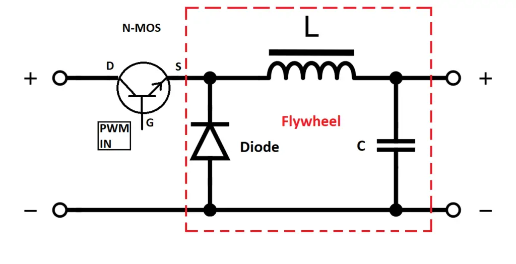
The above schematic is a generalized buck converter design, it consists of a transistor (practically it will be a MOSFET), a flywheel consisting of a schottky diode whose reverse recovery time is very small / can operate at high frequencies, an inductor with a ferrite core and an electrolytic capacitor.
A high frequency PWM controlled signal is required to make the above circuit functional; the input frequency at the base/gate of the transistor/MOSFET is in the range of tens of KHz to hundreds of KHz.
By controlling the duty cycle of the high frequency signal, we can control its output voltage. Higher the duty cycle higher the output voltage and vice-versa.
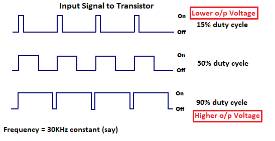
Also, higher the frequency smaller the physical size and values of the capacitor and inductor can be achieved. Utilizing SMD components are best for switching power supplies than through hole (THT) components because SMD components have less parasitic properties which leads to better efficiency, but in this project we will be only using THT components for better soldering convenience.
Working of buck converter (in layman terms):
Important properties of inductor: 1) Inductor opposes sudden / fast changes in the current. 2) It can store current in the form of magnetic field. 3) When the stored magnetic field collapses on the inductor (when the source removed) the polarity of generated current across the inductor is opposite to what source used to build magnetic field.
The working of a buck converter is better understood using two cases:
1) When the transistor is ON.
2) When transistor is OFF.
Transistor is ON:
When the transistor/MOSFET is turned ON the equivalent circuit will be as shown below:

- When the transistor is ON the current from input supply passes through the inductor, through the load and finally to the ground of the supply.
- Since the inductor doesn’t allow sudden changes in the current, the voltage across the load increases slowly (in micro-seconds time frame). The slow rise in voltage is due to the current across inductor is converted into magnetic field around it instead of supplying the current to the load.
- Once the slow rising voltage reaches our desire load voltage we will turn OFF the transistor. If we keep the transistor ON longer, the inductor will build its maximum magnetic field around it after which there will be no opposition in the current and output voltage will be equal to input source voltage which we don’t want to happen, but we need a lower voltage across the load than the source voltage.
- To do this as mentioned earlier we need turn off the transistor before the inductor could build its peak magnetic field around it. Meanwhile the diode is reverse biased and does not allow any current to pass through the diode.
- Now let’s continue understand what happens when we turn off the transistor.
Transistor is OFF:
When we turn off the transistor the equivalent circuit is shown below:
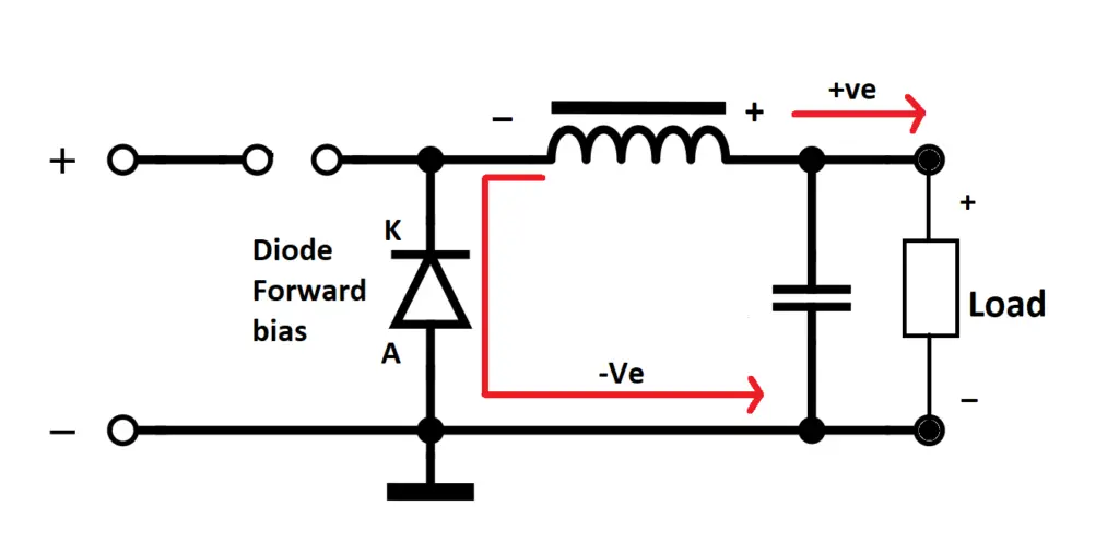
- Now the transistor is OFF and no current is passing through the inductor and the inductor can NO longer support the magnetic field around it, this leads to the collapse of magnetic field on itself.
- Now the inductor will act as a DC generator in the above shown polarity. If you take a closer look it is in opposite polarity to what was before (when transistor was ON).
- The –Ve supply potential across at the cathode terminal of the diode makes it forward biased and it reaches –Ve terminal of the load.
- Any fluctuations in the DC supply across the load are smoothed out by a capacitor while turning ON and OFF the transistor and also during when the inductor is building its magnetic field and discharging.
- The transistor will be turned ON again before the capacitor loses any significant charge to maintain a steady voltage across the load.
A point worth noting: Unlike linear voltage regulators where the excess energy is dissipated as heat to regulate its output, the buck converter stores its excess energy temporary as magnetic field and reusing it in next cycle is the key for its superior efficiency.
If you wish to learn more technical terms related to buck converter like continuous mode, discontinuous mode, synchronous rectification, multi-phase buck and its related calculations, please refer this Wikipedia resource page.
Designing a better switching stage for buck converter:
In this part we are going to make a simple alteration to the general buck converter design which will reduce designing complexity and improve efficiency greatly.
Take a note: N-channel MOSFETs are primarily made for switching –Ve supply rail and P-channel MOSFETs are primarily made for switching +Ve supply rail.

In theory the above circuit works and can be used for describing how a buck converter works, but practically the above circuit does not work properly without bootstrapping the MOSFET i.e. biasing the MOSFET properly with the help of additional circuit stage for switching high side (+Ve supply rail).
The problem with the above circuit is the MOSFET is an N-channel type which is switching high side (+Ve power rail) and the source terminal is just floating i.e. not fixed to 0V or GND. The input PWM signal cannot turn ON the MOSFET properly to switch the flywheel stage.
This design flaw came to light while we were prototyping the buck converter circuit and the MOSFET got very hot.
This issue was solved by simply rearranging the MOSFET as shown below:
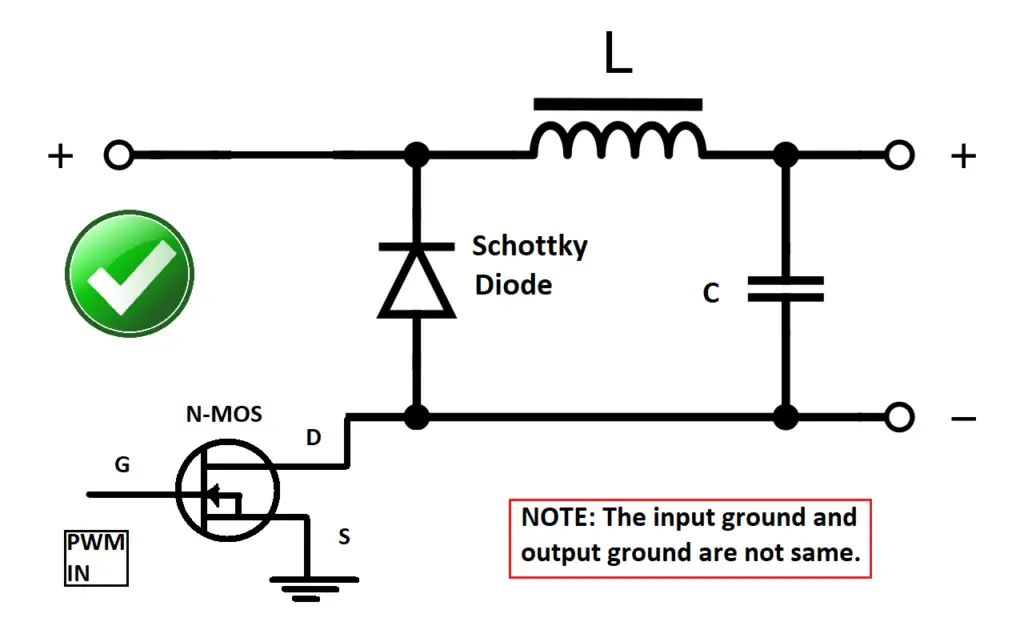
The MOSFET is now rearranged to switch low side (–Ve rail of the supply), precisely for what N-channel MOSFETs are primarily made for. Using this we were successfully able to step-down the voltage efficiently with least heating of MOSFET.
Note: The working explanation of buck converter does not change with this rearranged MOSFET configuration.
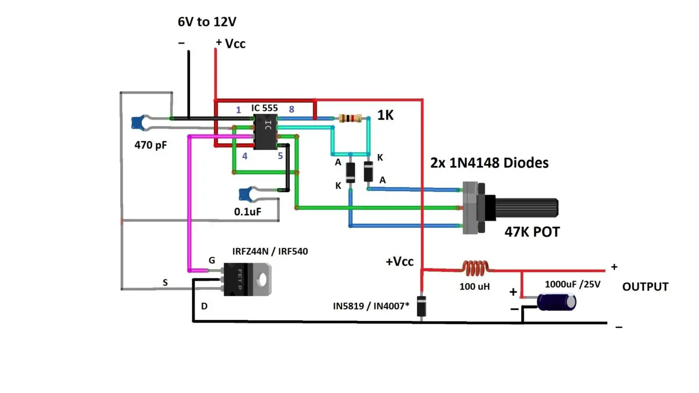
Full circuit diagram of buck converter using IC 555:
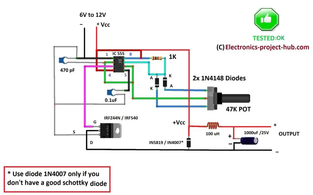
Note 1: Do not change the values of 470pF capacitor, 1K resistor, 47K variable and diode 1N4148. They are fine-tuned and tested for giving a smooth output.
Note 2: The absolute maximum input voltage is 15V above which IC 555 may get damaged.
Circuit description:
The oscillator IC 555:
The circuit consists of commonly available components; the heart of the circuit is an evergreen IC 555 which is configured as astable multivibrator which generates around 30 KHz frequency with the help of passive and active components connected to it.

As mentioned earlier we need to control the duty cycle of the frequency using which we can control the voltage at the buck converter’s output. Controlling / able adjust the duty cycle of an oscillator is called PWM control.
Fast switching diodes:
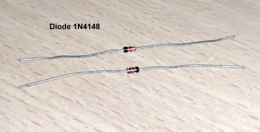
The PWM control is achieved by connecting two fast switching diodes (1N4148) anti-parallel to pin #7 of IC 555.
Capacitors:
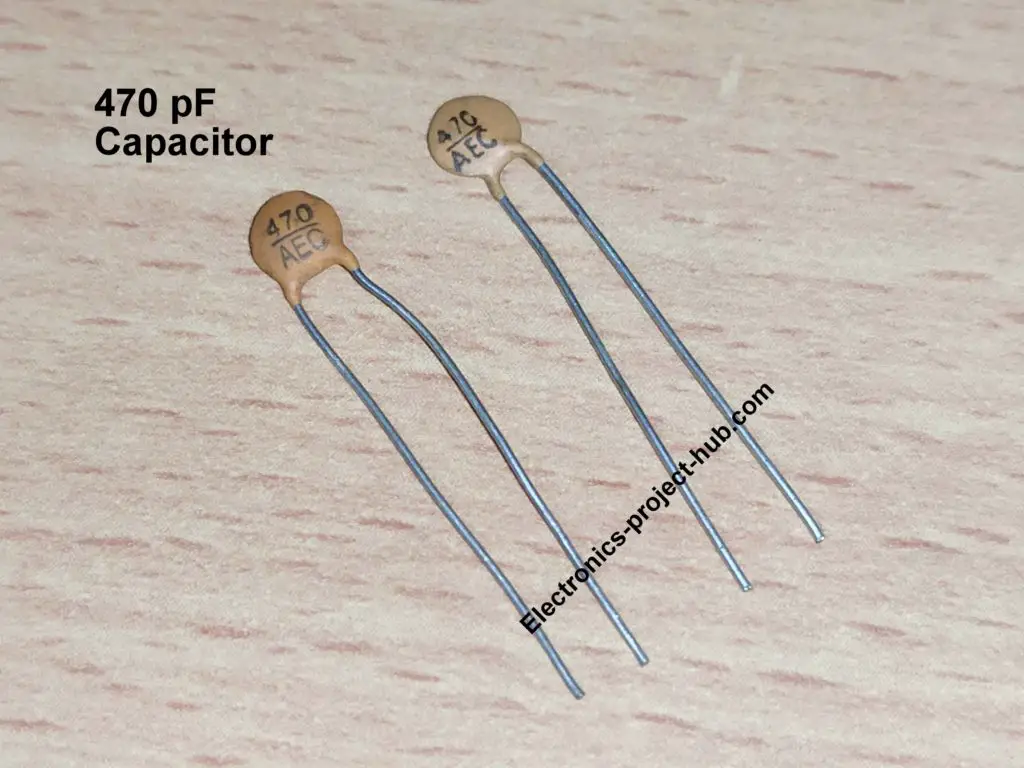
A 470pF capacitor is connected across pin #2 and GND, 470pF capacitor values are marked as 470 as shown below. Don’t omit the 0.1uF (104) capacitor connected at pin #5 they help in stabilizing the output and provide immunity against electrical noises.
N-channel MOSFET:
An N-channel MOSFET (IRF540 / IRFZ44N) is used as an amplifier which amplifies the faint signal from IC 555 and its gate terminal is directly connected to pin #3 of IC 555. The MOSFET switches the flywheel circuit at around 30 KHz.
The Flywheel circuit:
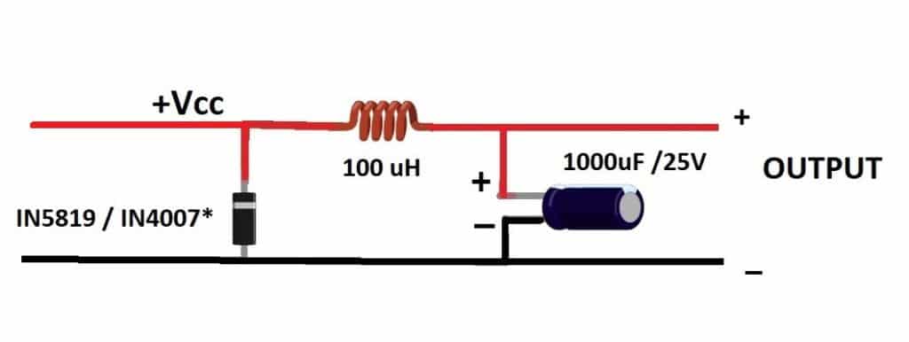
The flywheel circuit utilizes a schottky diode such as 1N5819 / 1N5822 which are designed for working at high frequencies. In the prototype we have used a general purpose rectifier diode 1N4007 because we ran out of schottky diodes but it worked just fine. When you make this circuit you should preferably use a schottky diode with at least 1A current capacity.
An inductor is connected between the diode and an electrolytic capacitor. The inductor is the key reason why the buck converter is so efficient; we have utilized a 100uH inductor and the value doesn’t have to be precise, slight variation in the value may not affect the output.
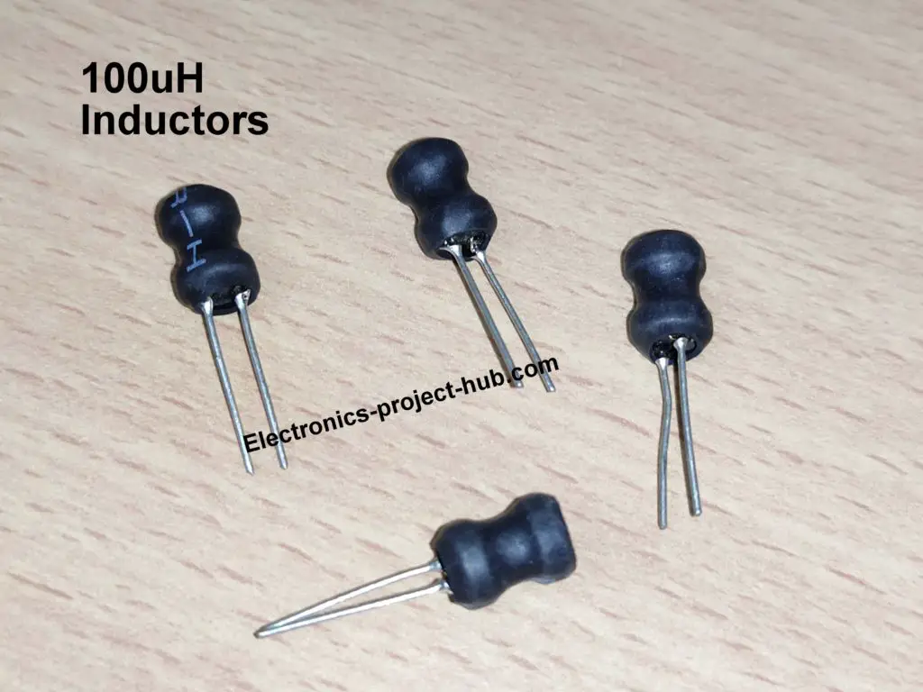
You may salvage an inductor or you may also purchase it from your local electronic stores / e-commerce sites.
Tested prototype:
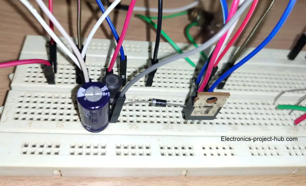
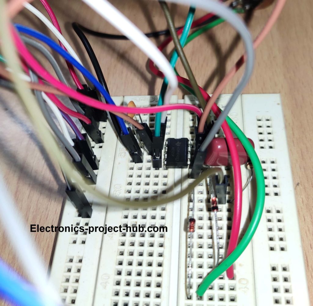
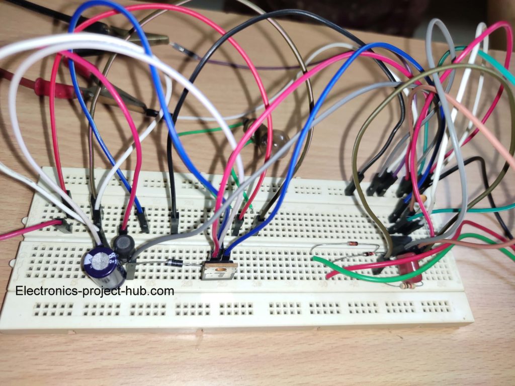
How to operate this buck converter correctly?
You must follow the instruction in the mentioned sequence:
- Connect the load at the output and a multimeter in VDC mode parallel the load.
- Keep the potentiometer at its minimum position initially.
- Power the buck converter now (6V to 12VDC).
- Gently rotate the potentiometer to increase voltage. Stop when your desire load voltage is attained and you are done.
- Always, the load should be connected at the output first before you power the buck converter ON.
- This is because there is no feedback system in this buck converter design and without any load the 1000uF capacitor will be charged equal to input voltage and if you connect a load now it has to bear the higher voltage for few milliseconds before the voltage drops to previously set value.
- This circuit is best suitable for fix loads meaning the power consumed by the load stays the same as long as it is powered ON.
If you have any questions regarding this project, feel free to ask us in the comment section and you will get a guaranteed reply from us.



This is nicely thought out and explained. It would be even nicer if it could be adapted to be closed loop based on the output voltage! Also, a way of setting a current limit with a potentiometer?
Thanks! If possible we will try to make another buck converter with closed loop circuit.
how did you arrive at these values for capacitor and inductor?
Hi,
I concluded the values of inductor and capacitor through my experience with electronics. First I tried with a value I thought it would work and check the output for ripples and distortions, if it worked fine keep the values, if it doesn’t work well fine tune the values till you get the correct output.
Regards
It seems like both the source and drain terminals of the IRF540N are connected to ground. Or am I missing something here.
Hi,
Can you please tell which circuit diagram you are referring to?
this circuit is not working.I have done the circuit and it’s not stable and not predictable.One more problem,the capacitors and resistors values are too small and circuit’s frequency is very high So can’t simulate the circuit because of frequency.Proteus is not capable to show the output voltage couse of the frequency.(If i did everything correct of course)
Hi,
The circuit is well tested one. The output is stable as long as the input voltage don’t vary or the load impedance vary.
The frequency must be high so that the components value can be small and the whole circuit can be packed in a small area.
Commercially made buck converters have frequency in the of MHz to reduce the size of the components and to increase maximum power output.
We will try to make a update with Porteous soon or later.
Regards
I’m also trying to build a Buck converter.
I have a 48 V voltage source, with which I want to charge a 36 V battery (42 V, full).
I would be interested in a converter that can withstand a current of 5 A.
I also saw some drawings on “[PROTECTED]”.
A 12V zener can be used at the input, for 555.
And the Mosfet transistor is powered from 48 V.
Thanks for the explanations.
Good luck..
Use a inductor that is rated for at-lest 6A, if your maximum current is 5A.
Regards
Bună ziua, am nevoie de ajutor,vreau să îmi arătați o schema dc dc converter 12v to 98v cu 30A, va rog foarte mult
English: Hello, I need help, I want you to show me a dc dc converter diagram 12v to 98v with 30A, please very much.
We are sorry, it is not possible for us to do as of now. We are very busy with other projects. We will try our best in future.
Ne pare rău, nu este posibil să facem acest lucru de acum. Suntem foarte ocupați cu alte proiecte. Vom încerca tot posibilul în viitor.
i am doing this for my part of project
could u provide me proteus simulation, i am having trouble simulating
Hi,
We haven’t made a simulation, we will be try to do it….
which diode is used in the prototype?
We used 1N4007 for the flywheel because we did not had a 1N5819 diode.
why cant i comment
well, you did it!
why my output only 10 V while my input is 12V and i think my 47k variable resistor is not working
Are you talking about a simulation or the practical build?
Can I use 50k variable instead of 47k?
Yes, you can.
How would i adjust the switching frequency in the circuit?
You can change the switching frequency by changing the values of 470pF, 1K resistor and 47K potentiometer.
First of all… Can I use a single 555 if to drive multiple irf540 MOSFET?
And can a preset be used in place of the potentiometer?
I’d appreciate a response. Thank you!
Yes! you can for both.
Can I use a single ne555 ic to multiple n channel MOSFETs(irf1404) which are in parallel?
And can a preset be used in place of the POT?
Yes!
After I tried that, output voltage isn’t regulate. Vout drop when the load connect. Which way can I solve?
Hi, sorry for the late reply.
The proposed circuit does not regulate the voltage and it is mentioned in the post, we will try to make one with voltage regulation soon or later.
Regards
Can i use p channel mosfet with npn transistor???
Use a N-channel MOSFET!
Can you share the simulation part breadboard part perfectly
My nickname is bigbrother.
hello, I stumbled across your site.
I looked at the schematic of your project and constructed it.
I use the circuit parts I currently have
Instead of capacitor 470PF, 430PF (221 ceramic capacitor in parallel connection) and FET IRF 630A were used.
The rest of the parts are configured according to your suggested circuit diagram.
The power supply voltage is 12V, the oscillation frequency is about 50kHz, and the average voltage of the output is 11.8V. It does not change the output even when the duty cycle is changed.
I have reviewed this circuit several times. Your project does not present an output waveform for changes in supply voltage and input duty cycle. No one knows the outcome of this project.
If time permits, by presenting the operating state of the circuit, the output change in response to the input change, You should try to solve the questions mentioned above.
I will also analyze the solution to this problem.
Hi,
Kindly read the operating instruction that I already mentioned in the article.
The reason why the output voltage doesn’t change when you vary the duty cycle is because the capacitor gets charged to Vpeak of the supply (when unloaded).
To prevent this you may connect a dummy load resistor of say 1K at the output and try varying POT, the output voltage also varies.
By the way this a tested circuit.
Regards
Well done Sir,
Please apart from the inductor what other things, need modification for high current. Is the schtoky diode handle high current.
Yes, the diode only if it does not suit your specification.
Lets say i want to give an 20V supply and not 12V. In that shouldnt i give 20v negative to the source of mostet?
Yes! Don’t apply more than 15V to the circuit.
It looks great!!
Can I use an input Voltage of 5 V, such as a cellphone charger? I need to convert it to 1.5 V 1 A…
Should I make any changes to the circuit?
Thanks in advance!!!
Hi,
Yes you can use 5V as input, but the efficiency may reduce by a lot and since the MOSFET require a higher GATE voltage to operate at better efficiency.
As long as you don’t consume huge current it should be fine.
regards