
Boost Converter Circuit Using IC 555
In this post we are going to design and simulate a (non-inverting) boost converter circuit using IC 555 and MOSFET which can supply a higher voltage than its input. The proposed boost converter circuit can operate from 5V to 15V and can output a variable voltage up to 40V. We will explore how a boost converter works, its computer simulation and video.
We will see:
- What is a boost converter?
- Boost converter v/s Buck converter.
- How a boost converter works?
- Boost converter circuit diagram and description.
- Simulation and video.
- How to operate this boost converter practically?
What is a boost converter?
Boost converter is a DC to DC step-up voltage converter whose output voltage is always greater than its input while its output current is lower than its input. It is a category of switch mode power supply or SMPS which can efficiently convert voltage from one level to another and its input and output power are ideally the same.
A basic practical boost converter circuit consists of two semiconductor and two energy storage components. The two semiconductor components are a switching MOSFET and a schottky diode; the two energy storage components are an inductor which plays a key role in boosting voltage and a capacitor to smooth the DC output.
Boost converter v/s Buck converter:
The boost and buck converters perform complimentary functions yet most of their utilized components are the same, only their arrangement make them boost or buck. Let’s do a comparison and understand their similarities and differences.
| Parameters | Boost Converter | Buck Converter |
|---|---|---|
| Voltage: | Always higher than its input. | Always lower than its input. |
| Current: | Always lower than its input. | Always higher than its input. |
| Power: | Input and output power is ideally the same. | Input and output power is ideally the same. |
| Voltage varied / controlled by? | PWM input | PWM input |
| Role of inductor : | To boost output voltage by connecting the stored energy in series with input supply. | To reduce input voltage by storing excess energy to inductor and reusing it in next cycle. |
| Input / output Isolation: | No galvanic isolation exists between input and output. | No galvanic isolation exists between input and output. |
| Types: | Inverting and non-inverting. | Inverting and non-inverting. |
| Applications: | Battery operated devices, solar chargers, flash lights, transformerless inverters etc. | Battery operated devices, step-down regulated power supplies in TV, PC, battery chargers etc. |
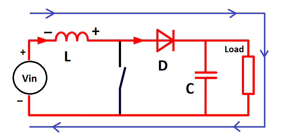
General schematic of (non-inverting) boost converter:
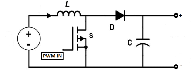
The above schematic is a generalized non-inverting boost converter; it is called a non-inverting boost converter because its input and output polarity sides are the same. The above circuit consists of an N-Channel MOSFET, an inductor, a reverse blocking diode and an electrolytic capacitor; these four (main) components do the job of boosting and smoothing of output.
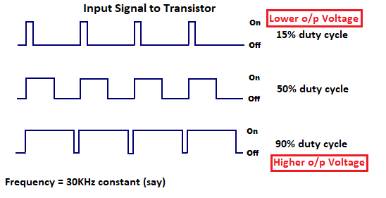
To make the above circuit work we need to apply a high frequency signal in the range of tens of KHz whose duty cycle can be varied. The duty cycle is going to determine the output voltage. If the duty cycle is low the output voltage will be low but higher than its input and if the duty cycle is high the output will be way higher than its input.
Working of boost converter (simplified for layman):
Pre-knowledge on inductor: 1) Inductor opposes sudden / fast changes in the current. 2) It can store energy in the form of magnetic field. 3) When the stored magnetic field collapses on the inductor (when the source removed) the polarity of generated current across the inductor is opposite to what source used to build its magnetic field.
The working of boost converter can be understood better using two scenarios:
- When the MOSFET is ON.
- When the MOSFET is OFF.
MOSFET ON:
When the MOSFET is ON, the equivalent circuit will be as shown below:
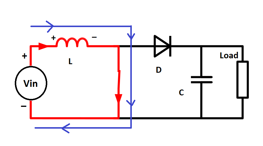
- When the MOSFET is ON, current passes through the inductor, through the MOSFET and finally to the ground.
- As mentioned earlier the inductor does not allow sudden changes in the current, meaning when the MOSFET is ON inductor won’t allow full current from the input to pass through the MOSFET and to the GND, instead the current will rise slowly in micro-second time frame.
- The slow rise in the current is due to the inductor converting the current in to magnetic field around it. Once the magnetic is fully built around it there will be no opposing in the current flow (the MOSFET will be turned OFF before the inductor fully built its magnetic field, because it will cause short circuit).
- When the inductor has built sufficient magnetic field around it in the above shown electrical polarity the MOSFET will be turned OFF. Let’s continue understand what happens when MOSFET is turned OFF.
MOSFET OFF:
The equivalent circuit when the MOSFET is turned OFF is shown below:
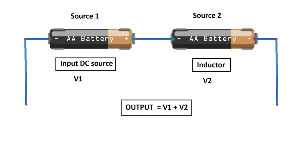
- When the MOSFET is turned OFF fully, the inductor can no longer support its magnetic field around it, so it collapses on the inductor itself and act as a DC generator in the above shown electrical polarity (which is opposite to what the input supply built its magnetic field).
- Now if you take a look at the above circuit, you will observe that the generated voltage across the inductor is in series with the input voltage, these two voltages add-up like when two cells connected in series, now the output will be sum of the two voltages.
- This higher voltage is passed through a diode and charges an electrolytic capacitor. The diode prevents the charge flowing backward and ensures the stored charge is passed to a load connect at the output.
- The MOSFET is turned ON again before the capacitor loses any significant amount of charge to maintain a steady voltage across output.
If you wish to learn more about boost converter and its related technical terms like continuous mode, discontinues mode and its related mathematical calculations, please refer this Wikipedia resource page.
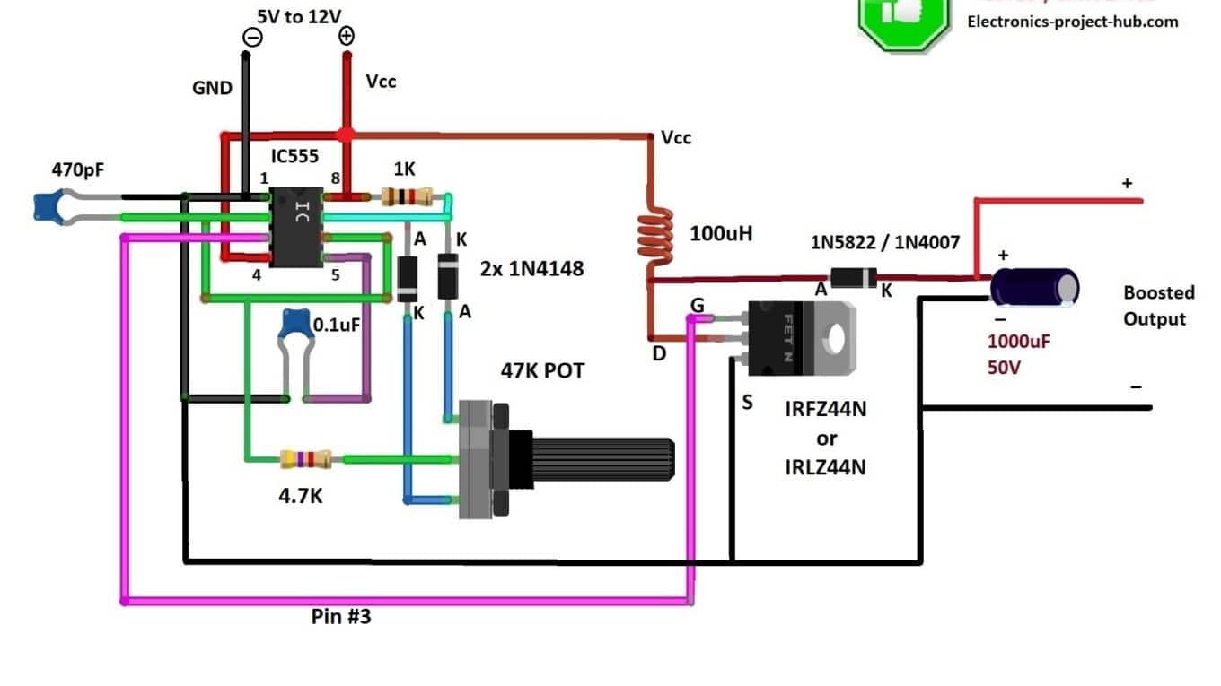
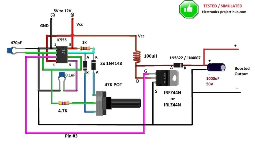
Full circuit diagram of boost converter:
NOTE: The absolute maximum input voltage is 15V above which MOSFET / IC 555 may get damaged.
Circuit description:
The above circuit can be constructed using commonly available active and passive components. The above circuit consists of two stages: the oscillator and boosting stage let’s explore them in detail.
IC 555 oscillator:
The evergreen IC 555 is configured in astable multivibrator mode, which oscillates at around 30 KHz with the help of RC components connect around it.
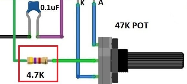
To control the output voltage we need to control IC 555’s duty cycle, to accomplish this two fast switching diodes 1N4148 are connected anti-parallel between pin #7 and a 47K potentiometer, by rotating the potentiometer clock and anti-clockwise we can adjust its duty cycle and so does boost converter’s output voltage.
Role of 4.7K at the output of potentiometer: A 4.7K resistor is connect to 47K potentiometer’s output terminal to limit the IC 555’s duty cycle to 90%, this is very important because if a user rotates the knob fully, the output will get saturated i.e. 100% duty cycle.
At 100% duty-cycle the MOSFET is ON continuously and creates full short circuit via inductor.
We also found using simulation that approximately above 90% duty-cycle the output voltage did not raise but reduced significantly, this could be because the MOSFET is ON for too long and not enough time for the inductor’s magnetic field to collapse and generate a voltage across it.
Booster stage:
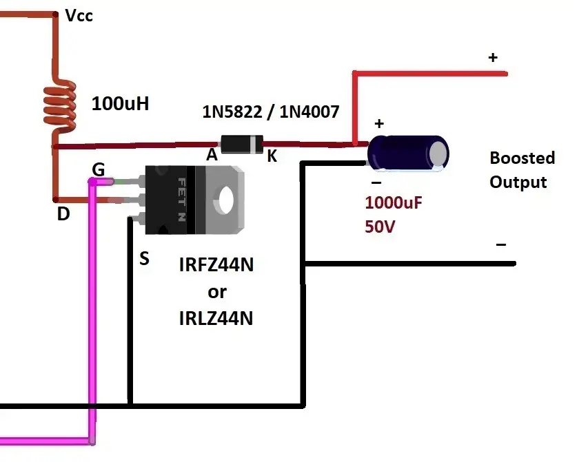
The booster stage is exactly same as the general boost converter circuit that was shown earlier in this post, now we have to give a fixed value to each of the components.
MOSFET:
The recommended MOSFET for this boost converter is IRLZ44N (not to be confused with IRFZ44N), IRLZ44N is a logic level MOSFET which can fully turn ON at 5V (Vgs), we need such lower GATE voltage because as a boost converter circuit we’ll be applying a lower voltage like 5V/6V to extract a higher voltage from it, at these lower voltages other general purpose MOSFET won’t fully turn ON.
If you didn’t have an IRLZ44N MOSFET you can substitute with IRFZ44N MOSFET, the circuit still works, but there will some efficiency losses.
Diode:
The booster circuit has a schottky diode which prevents the charge stored in capacitor flowing back to inductor and ensures the boosted voltage passes to electrolytic capacitor and load.
The recommended diode is 1N5822 which is a fast switching schottky diode designed to operate at higher frequencies like this and also it has a lower forward drop voltage which contributes to greater efficiency.
You can also use a silicon diode 1N4007 in case you don’t have a schottky diode, but there will be efficiency losses.
Capacitor:
We are using a standard electrolytic capacitor with voltage rating of at-least 50V; this is because the proposed boost converter circuit at no load condition can shoot well above a pre-set voltage and the capacitor needs to withstand it.
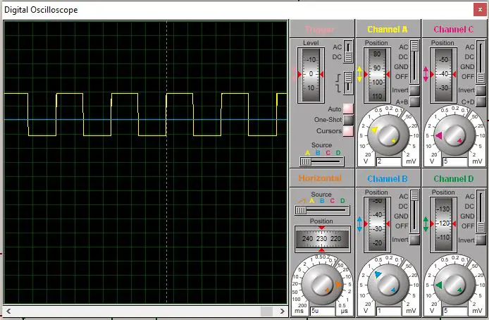
Boost converter simulation:
Click here to download Proteus simulation files.
Circuit diagram on Proteus simulation software:

Duty cycle on virtual oscilloscope:
How to operate this boost converter practically:
The proposed boost converter can not only built on simulation software but also can be built practically. If you are building this boost converter, here are the correct ways to operate this circuit:
- Initially keep the potentiometer’s knob at minimum.
- Connect the load at its output and connect a DC voltmeter across the load.
- Now power ON the boost converter circuit.
- Gently rotate the potentiometer to increase the voltage, once the desire voltage is reached stop rising further.
- When you turn ON the circuit next time with the same load, the circuit will output the same voltage as you set previously.
- The boost converter should be turned ON only after the load is connected at its output first, this is because at no load the output voltage shoots up a lot and connecting a load now may damage it.
- This boost converter is best for fixed loads, meaning the load’s power consumption stays steady always.
If you have any questions regarding this post feel free as us in the comment, you will get a guaranteed reply from us.
Blogthor
My nick name is blogthor, I am a professional electronics engineer specialized in Embedded System. I am a experienced programmer and electronics hardware developer. I am the founder of this website, I am also a hobbyist, DIYer and a constant learner. I love to solve your technical queries via comment section.


Ic 555 must be CMOS type other wise ne555 TTL ic will not work in 5v vdc
Hi,
CMOS IC555 is a good substitute for this circuit and also a normal TTL can operate from 4.5V.
Regards
I want sine wave bust in this circuit please explain me how do it ???
Hi, Could you please elaborate your question more?
How to make a inductor .i made ring ferrite core with 25T with 0.8mm wire.core diameter is 26mm.
Hi,
Sorry for late reply. You can certainly try with your coil build, but we recommend a ready made one.
Regards
hello blogthor, thankyou your works is very useful. hope you’re all good during this pandemic.
and for this project, what should i do if iwant a higher voltage?
Hi,
Thanks, I hope you really enjoyed learning it.
The easy way to increase output voltage is to increase the input voltage (limit less than 15V) the other possible method is increasing the frequency (speaking generally).
Regards
hi, yes i doit just for fun.
I actually try to replace this contact breaker (S1) with your circuit of swithcing.
Regards
can i run with 8 (1.5V) batteries
As long as the input voltage is less than 15V, you are fine.
Very good project please can you tell maximum output ampere if at input I am using 6 volt 4ampere and I need 12 volts at the output ( please tell maximum Load ampere at output)
Hi,
You may get 2 ampere minus the losses. Make sure your inductor can handle the current.
Regards
Can I replace POT 47K with POT 50k?
Yes, you can!
can we design the same circuit using op-amps (LM324 or similar) instead of IC555
Yes you can, but the op-amp must be configured as astable multivibrator.
what will be the output voltage; I cant determine it on your circuit diagram
Hi, the output is variable!
Can I load 10 ampere for the input ?
Your input source must be capable of providing of more the 10 amps is the basic requirement. When you increase the voltage the current drops at the output. For 10 Amps output, connect multiple MOSFETs of the same part number in parallel.
Can i use this to build a 12V input 3A input to a 36V ouput and about 1Amp ouput with a duty cycle of 0.67 and switching frequency of 20kHz using an ne555
Hi,
Sorry for the delayed reply.
Yes you can, make sure that your load consumes a constant power from the boost converter.
Regards
what is the duty cycle, ripple current, input voltage and output voltage assumed for this circuit ?
Hi,
The duty cycle is from 0 to 99%, ripple current is minimal (DC) as far as we can say, input voltage is 5 to 12V, output voltage depends on the potentiometer.
Regards
will this circuit can be used on LTSPICE because i am facing trouble in making potentiometer (as it is not available in its library).. can u pls give me hint how to proceed.
The circuit should work on LTspice, but I am not sure about the POT, please get help from someone who knows better about LTspice than us.
Hi
Will ne555 work well in place of ic555?
How can i get an output current of 5-8 Amps @20v with an input supply of 8v 2Amps?
Thanks
Hi,
You can use NE555 which is essentially same as IC555.
You cannot get more output than you put into the circuit. If the voltage increases the current must decrease, this is universally true for all the machines.
Regards
Why the MOSFET gets very hot and burn out even when there is no load?
Hi,
Your MOSFET is probably getting burnt because the MOSFET is fully ON all the time making short circuit from GND to +Ve via inductor and this could be because the IC 555 is not generating the squarewave, instead pin #3 is outputting HIGH all the time. You can test it by using your multimeter in DC mode and when you vary the POT you should get varying voltage at pin #3 depending on POT’s position.
Regards